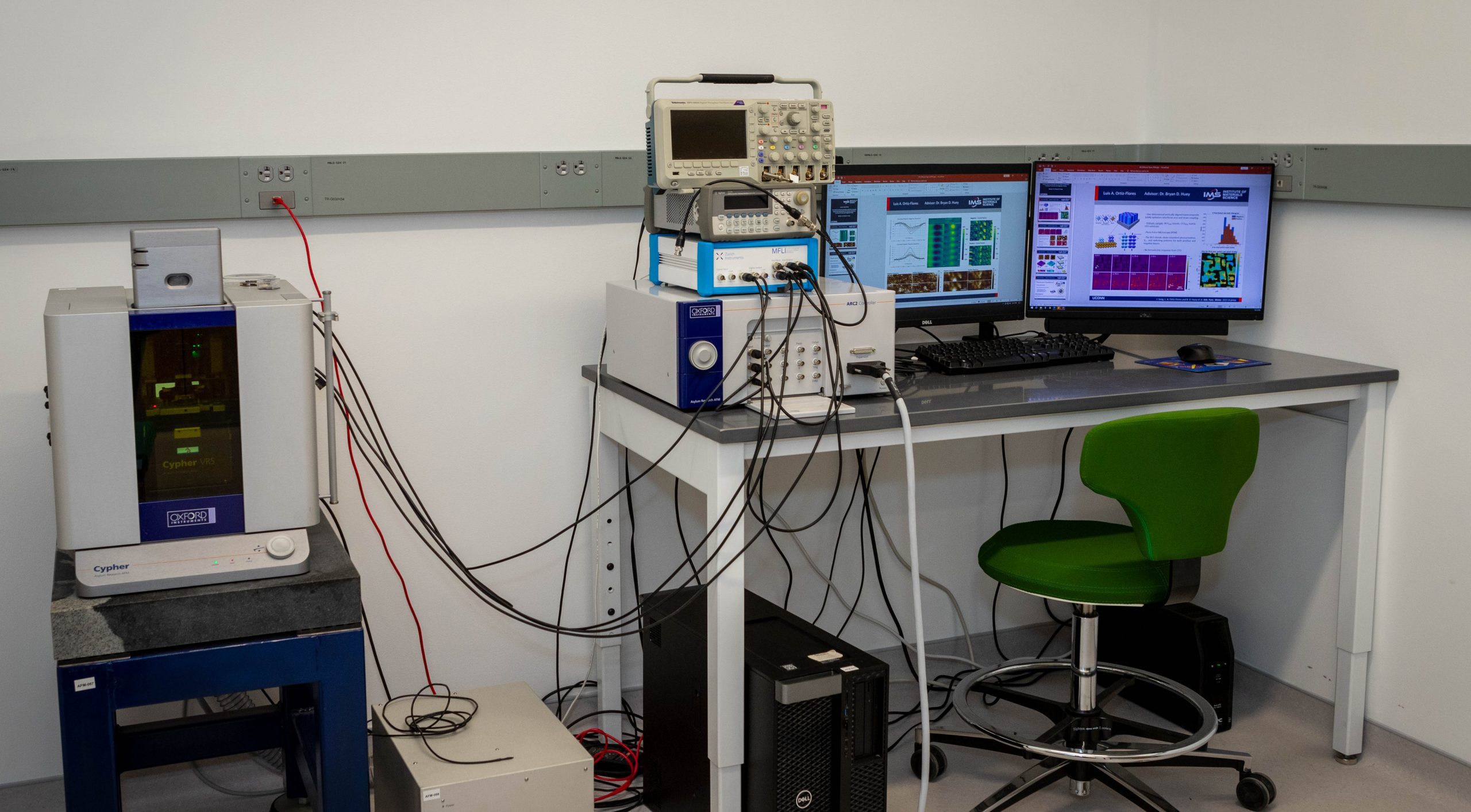
Available Methods and Accessories
The AFM user facility residing within IMS excels at multiple advanced characterization methods. Lab personnel have substantial expertise with a wide range of novice to expert AFM techniques that utilize creative methods to achieve imaging needs.
Accessories include VR high speed scanner, dual gain ORCA for CAFM, high V module for TDDB, and all hardware and software for nanolithography, contact and AC mode (‘Tapping’) imaging, and contrast mechanisms spanning phase, CAFM, pcAFM, EFM, MFM, SSPM/KPFM, PFM, AFAM, FFM, and F-d measurements and mapping.
Sample Requirements
Optimal samples up to 7mm by 7mm (xy) and 5mm (z). Up to 1cm by 1cm (xy) and 6mm (z) can be accommodated, but area of interest must be centered. Samples will be fixed to a magnetic disk.
Summary of Technique
AFM can provide high resolution imaging of the surface topography, and for certain specimens also local materials properties. These can include phase, current, photocurrent, electric fields, magnetic fields, surface potential, piezoresponse, mechanical compliance, friction, adhesion, and stiffness. Tomographic AFM and high speed AFM may even be feasible for certain applications.
Note AFM is generally slow and difficult, requiring many hours for quality data and tens of hours of practice to begin to master.
Information Provided & Detection Limits
Max scan range = 30µm by 30µm (xy) by 5µm (z).
Typical realistic resolution (accommodating tip contact area and depending on contrast mechanism) is atomic to 50 nm (xy) and a few Angstroms in (z). For oscillating signals, pm resolution is practical.
Common results: Images, point measurements, roughness calculations, height or property histograms. Original data format: Wavemetrics Igor (.ibw).
Lab Location and Contact Information
Lab Location: AFM user facility, Science1, G024
Lab Manager: Professor Bryan Huey
bryan.huey@uconn.edu
860-486-3284