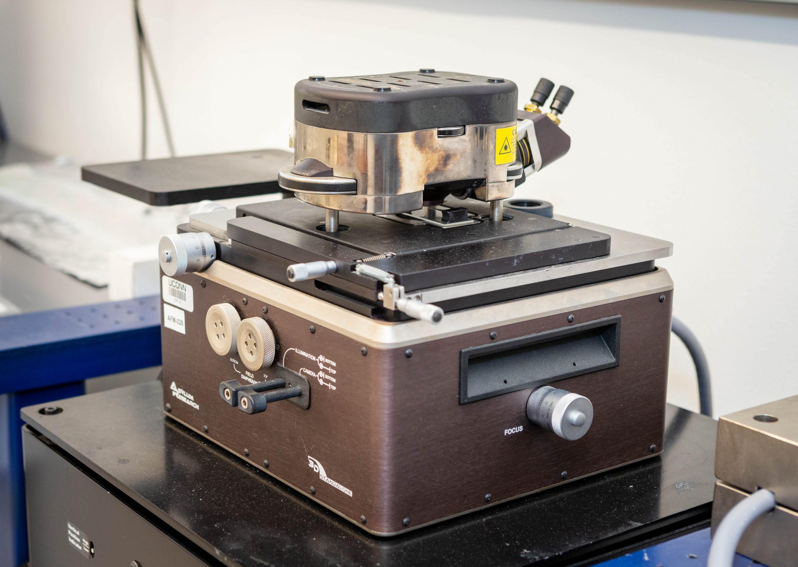
Available Methods and Accessories
The AFM user facility residing within IMS excels at multiple advanced characterization methods. Lab personnel have substantial expertise with a wide range of novice to expert AFM techniques that utilize creative methods to achieve imaging needs.
Accessories include POLY-heater for variable temperature AFM (RT up to 300C), humidity control via salt solutions, and all hardware and software for nanolithography, contact and AC mode (‘Tapping’) imaging, and contrast mechanisms spanning phase, CAFM, pcAFM, EFM, MFM, SSPM/KPFM, PFM, AFAM, FFM, and F-d measurements and mapping.
Sample Requirements
Conventional AFM: Optimal samples up to 1cm by 1cm (xy) and 5mm (z). Up to 5cm by 5cm (xy) and 2cm (z) can be accommodated under certain conditions. Samples will be fixed to center of a standard glass microscope slide (25mm by 75mm).
Summary of Technique
AFM can provide high resolution imaging of the surface topography, and for certain specimens also local materials properties. These can include phase, current, photocurrent, electric fields, magnetic fields, surface potential, piezoresponse, mechanical compliance, friction, adhesion, and stiffness. Tomographic AFM may even be feasible for certain applications.
Note AFM is generally slow and difficult, requiring many hours for quality data and tens of hours of practice to begin to master.
Information Provided & Detection Limits
Max AFM scan range = 100µm by 100µm (xy) by 15µm (z).
Typical realistic resolution (accommodating tip contact area and depending on contrast mechanism) is 1to 50 nm (xy) and a few Angstroms in (z). For oscillating signals, tens of pm resolution is practical.
Common results: Images, point measurements, roughness calculations, height or property histograms. Original data format: Wavemetrics Igor (.ibw).
Lab Location and Contact Information
Lab Location: AFM user facility, Science1, G024
Lab Manager: Professor Bryan Huey
bryan.huey@uconn.edu
860-486-3284